JTAG is a physical hardware interface that makes it possible, among other things, to extract the firmware image from electronic devices.
The firmware, a program that executes in a dedicated way and with a specific purpose in a microcontroller or microprocessor, is usually stored in a persistent memory device like a NAND/NOR flash or EEPROM.
The extraction process involves reading and copying the firmware image stored in the device’s memory to a file on your computer. This process of extracting the firmware image is also called dumping or snarfing.
But why extract the firmware from an electronic device?
Why?
Imagine an electronic device like a router, an IP camera or a hard disk.
Now imagine that you want to understand better how the device works, but you don’t have much information about it. Extracting and analyzing the firmware image can be a viable option to understand its operation.
You may want to improve or change the behavior of the device. Without access to the source code, one possibility is to extract the firmware to make the necessary changes and then update the device.
What if you forgot your credentials and lost access to the device? One possibility to regain access is to extract and change the firmware image.
If you are a security researcher, you may want to extract the firmware of the device to look for vulnerabilities in the software.
And what if the device is very old and is no longer being manufactured or sold by the vendor? You may want to clone it, and extracting the firmware image will be essential in this process.
As we can see, there are many situations that can motivate us to extract the firmware from an electronic device. Even if it’s just for fun!
Firmware extraction techniques
Several techniques can be used to extract the firmware from an electronic device.
But before you start, make sure the firmware image is not available on the manufacturer’s website. Many device manufacturers such as routers and cameras publish updated firmware images on their websites, so that customers can download and update the device. In this case, the effort to extract the firmware is zero!
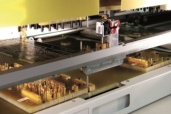
With physical access to the device, a technique for extracting the firmware is to directly read the device’s storage memory. We can identify and remove the memory chip from the board, solder it on another board and extract the firmware. It works, but can be quite painful and maybe a little risky (there is a possibility of burning the memory chip during the extraction process).
A less risky technique is to simply read the device’s storage memory through a connection to the bootloader or operating system of the device.
For example, with access to the bootloader (via a serial connection), we can try to read the device’s memory and send the data to our machine. Likewise, with access to a command line terminal in the operating system (serial, ssh, etc.) and with privileges, we can try to dump the storage memory of the device and send it to our machine.
As we can see, different techniques can be used to extract the firmware from a device, depending on the situation.
And if none of these techniques are viable, the JTAG interface may be a good option!
What is the JTAG interface?
In the past, tests on PCBs (Printed Circuit Boards) were done through a system called bed-of-nails.
In this system, the PCB was designed with several test points to be connected to a test board. And this test board performed several checks on the connections and electronic components of the board.
As the complexity of a PCB increased, it started to get difficult and complicated to design a bed-of-nails for it.
Then some debug and test interfaces integrated into the chips (processor, microcontroller, SoC, FPGA, etc.) started to appear.
Exactly for this purpose, in 1985 the JTAG (Joint Test Action Group) interface was created, a standard (IEEE 1149.1) to test printed circuit boards during manufacture.
Over time, JTAG has become one of the most popular interfaces to test electronic circuits, getting other features like debugging and burning flash devices.
Currently, this interface is available in most processors and microcontrollers of different architectures such as ARM, x86, MIPS and PowerPC.
How does the JTAG interface work?
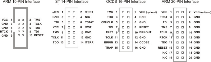
Although there are some variations of the standard, the JTAG interface is usually implemented by the chip manufacturer via four mandatory pins (TDI, TDO, TCK, TMS) and one optional pin (TRST):
- TDI (Test Data In): data input.
- TDO (Test Data Out): data output.
- TCK (Test Clock): clock whose maximum frequency depends on the chip (usually from 10MHz to 100MHz).
- TMS (Test Mode Select): pin to control the JTAG state machine.
- TRST (Test Reset): optional pin to reset the JTAG state machine.
The pins of the JTAG interface are internally connected to the chip through a module called TAP (Test Access Port).
The TAP interface implements the basic JTAG communication protocol, and several TAPs can be connected simultaneously in a daisy chain architecture.
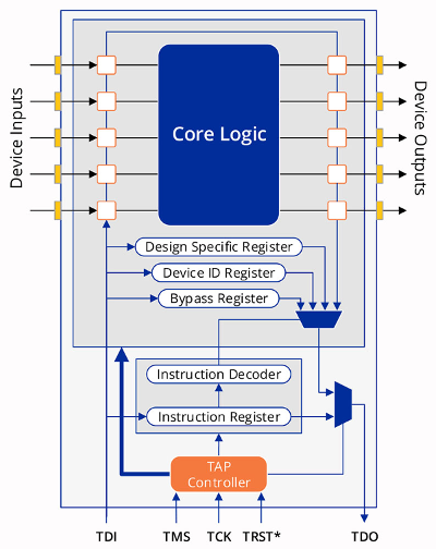
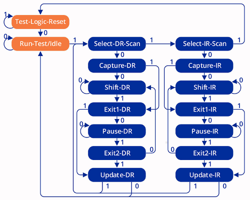
The TAP interface implements a finite state machine (16 states) that allows access to a group of registers (IR, DR) to instrument the chip. The control of this state machine is done through the pins TMS and TCK. Through this state machine, it is possible to select an operation via the IR register (Instruction Register) and pass parameters or check the result via the DR register (Data Register).
The size of the IR register and the number of instructions supported is defined by the chip manufacturer. For example, a 5-bit IR register will support up to 32 instructions.
Each instruction has its own DR (Data Register), which has a variable size. Three instructions are defined by the JTAG standard and must be implemented by the manufacturer (BYPASS, EXTEST, SAMPLE/PRELOAD). Other instructions are optional, but are also usually implemented (eg, IDCODE).
- BYPASS: instruction that selects a 1-bit register that rotates from TDI to TDO, very useful for testing the JTAG interface.
- EXTEST: instruction that selects the BSR (Boundary Scan Register) to read and change the state of the pins.
- SAMPLE/PRELOAD: instruction that selects the BSR register (Boundary Scan Register) to read the status of the pins.
- IDCODE: instruction that selects the device ID register (32 bits) that contains the chip ID.
In addition to the instructions defined by the standard, the chip manufacturer can implement other instructions as needed. In this way, many manufacturers extend the JTAG interface with debugging and memory access functions (eg: MIPS EJTAG).
Information about supported JTAG instructions and the pins on a chip is usually documented in a file called BSDL (Boundary Scan Description Language), a subset of VHDL (VHSIC Hardware Description Language).
For example, here’s a short excerpt from the STM32F1 BSDL available on the ST website. As we can see in the line 29, the JTAG interface of this microcontroller supports up to 32 instructions (5 bits).
|
|
Now that we know a little bit about the JTAG interface, what can we do with it?
The JTAG interface in practice
With JTAG we can control the execution of the firmware (stop the execution, inspect the memory, configure breakpoints, execute the code step-by-step, etc). We can also inspect the state of the processor and its registers, read and write to memory and access any I/O device connected to the processor.
Through a feature called Boundary Scan, the JTAG interface allows access to all the pins of the chip! In this way, we can individually read and write to each pin, and consequently manipulate the peripherals connected to the processor/microcontroller (GPIO, memory, flash, etc).
In practice, with the JTAG interface we can:
- Identify information about the hardware (processor, memory, etc).
- Dump RAM and gain access to sensitive data such as passwords and cryptographic keys.
- Change the behavior of programs at run time to obtain privileged access to the system.
- Capture sensitive data from hardware devices, such as information stored in an EEPROM.
- Activate peripherals and change their behavior, such as setting or resetting an I/O pin.
- And of course, dump the flash memory to extract the firmware of the device!
As we can see, the JTAG interface is perfect for inspecting the execution of the firmware, find vulnerabilities and exploit the device.
But if the JTAG interface is so insecure, why don’t many hardware manufacturers remove or disable the access to it?
Because the JTAG interface is very convenient for the development and production of the hardware! Developers use the JTAG interface to debug the firmware running on the device. Also, the JTAG interface is used as a tool for programming and testing the device in production.
However, some manufacturers may adopt countermeasures to make it difficult to use the JTAG interface in the final product, including:
- Obfuscation (cutting tracks, removing resistors, etc).
- Reconfiguration of the JTAG pins in software.
- Encryption and signature validation of the firmware image.
Other manufacturers go further and completely disable the JTAG interface through some fuses (internal bits of the chip that, once programmed, can no longer be changed).
Even so, it is still possible to re-enable the JTAG interface with techniques such as a silicon die attack.
After all, security is always a matter of how much time, knowledge and resources you have, right?
Now let’s get down to business!
Extracting firmware with JTAG
These are the four main steps to extract the firmware from a device using JTAG:
- Identify the JTAG connection pins.
- Test the connection with a JTAG adapter.
- Gather information about the memory mapping of the chip.
- Extract the firmware from the flash memory.
While explaining the process, I will provide a real example, extracting the firmware of the Linksys WRT54G router.
Step 1: Identify the JTAG pins
Finding the JTAG interface signals and their pinout can be quite laborious! That’s because the device manufacturer can hide, obfuscate or disable the JTAG interface.
But before you start, do some research. Maybe someone else has already identified the JTAG interface of your device and published on the Internet.
If you can’t find anything on the Internet, take the board of your device and look for a group of pins together and not populated through visual inspection. The pins of the JTAG interface may be hidden under some other component like a capacitor or a battery. Pay attention to the different standards of JTAG connectors (2x10, 2x8, 2x7, 2x5, etc).
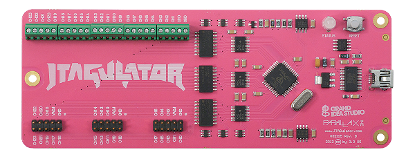
Download the datasheet of the processor to identify the JTAG pins and test with a multimeter, oscilloscope or logic analyzer. A brute-force tool like JTAGulator can also be very useful!
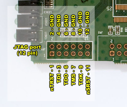
Sometimes the JTAG interface is quite evident and documented on the Internet, like that of the WRT54G router:
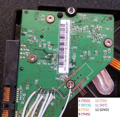
But sometimes it’s not that obvious, like the JTAG interface of this Western Digital hard drive:
Therefore, the process of identifying the JTAG interface can take some time and will require a lot of patience!
Step 2: Test the JTAG connection
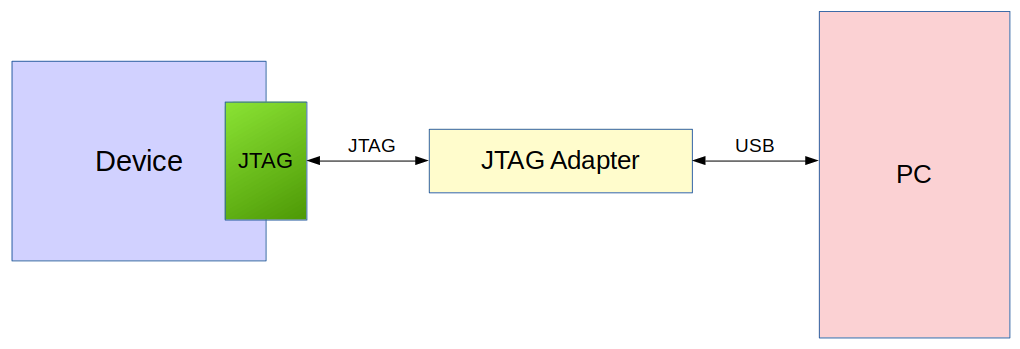
With the JTAG pins identified, we can start the communication process with the JTAG interface. For that, we basically need two components: a JTAG adapter and a JTAG communication software.
The JTAG adapter is responsible for the physical communication with the device through the JTAG interface, usually connecting to the PC via a USB interface.
The JTAG communication software is responsible for communicating with the JTAG interface through the JTAG adapter.
There are several JTAG adapters available on the market, some quite expensive for professional use and others more accessible, some of which are open hardware:
- SEGGER J-Link
- Keil ULINK
- Flyswatter/Flyswatter2
- Bus Blaster
- Bus Pirate
- Black Magic Probe
- Shikra
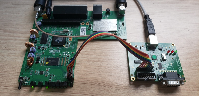
In my tests, I am using Flyswatter from Tin Can Tools. This is my setup:
To communicate with the JTAG interface, there are several software options, many of which are proprietary. Among the open source tools, we have OpenOCD and UrJTAG.
OpenOCD (Open On-Chip Debugger) is an open source tool for communicating with JTAG interfaces. The project has been around for many years, connects easily to GDB and has a very comprehensive support of JTAG adapters and hardware devices.
UrJTAG is a newer tool, simpler but with a more friendly interface.
In my tests, I will use UrJTAG, which can be easily installed in a Debian-based distribution:
$ sudo apt install -y urjtag

$ jtag

UrJTAG 0.10 #2007
Copyright (C) 2002, 2003 ETC s.r.o.
Copyright (C) 2007, 2008, 2009 Kolja Waschk and the respective authors

UrJTAG is free software, covered by the GNU General Public License, and you are
welcome to change it and/or distribute copies of it under certain conditions.
There is absolutely no warranty for UrJTAG.

warning: UrJTAG may damage your hardware!
Type "quit" to exit, "help" for help.

jtag>
With the JTAG adapter connected to the WRT54G, we can use UrJTAG to test communication with the JTAG interface and extract the device ID using the IDCODE instruction (this ID is a unique number assigned by JEDEC to each chip model manufactured in the world).
As we can see in the output below (line 7), the device ID of the WRT54G chip is 0x0535217F.
|
|
Step 3: Identify information about flash memory
The next step is to analyze the memory address space of the chip to identify the device’s flash memory initial address and size.
Visual inspection can help to identify the flash memory chip. Searching the Internet for information about the hardware platform or products with similar hardware can also help, as well as the documentation of the chip (SoC, processor, etc).
If you have access to a command line terminal on the device, look in the bootloader or the operating system logs for any message regarding the model and address space of the flash memory.
Sometimes it is necessary to apply some trial and error method or brute force to identify the address of the device’s flash memory.
In my case, as I am using a MIPS based router, I can try the EJTAG instructions (a MIPS extension of the JTAG protocol) to identify the memory mapping of the chip. From the output below, we can see that the flash address of the device is 0x1FC00000 (line 19).
|
|
With this address, we can use the detectflash command to collect information about flash memory. From the output below (line 19), we can see that the flash memory size is 4M:
|
|
Now we have all we need (flash memory start address and size) to extract the firmware from the device.
Step 4: Extracting the firmware
To extract the firmware, we just need to use the JTAG communication software to read the memory range identified in the previous step and save the data to a file.
Depending on the size of the flash memory and the communication speed of the JTAG interface, the process can take several minutes!
With the UrJTAG tool, we can dump the flash memory’s content using the readmem command:
jtag> readmem 0x1fc00000 0x400000 flash.bin
address: 0x1FC00000
length:  0x00400000
reading:
addr: 0x20000000
Done.
After several minutes, we will have the firmware image extracted from the flash memory of the device!
$ ls -lh flash.bin
-rw-r--r-- 1 sprado sprado 4,0M fev 18 22:12 flash.bin
Now we can analyze the firmware image of the router with binwalk:
$ binwalk --signature flash.bin

DECIMAL       HEXADECIMAL     DESCRIPTION
--------------------------------------------------------------------------------
211412        0x339D4         Copyright string: "Copyright (C) 2000,2001,2002,2003 Broadcom Corporation."
234095        0x3926F         Copyright string: "Copyright 1995-1998 Mark Adler "
239104        0x3A600         CRC32 polynomial table, little endian
262144        0x40000         TRX firmware header, little endian, image size: 3211264 bytes, CRC32: 0xA293EEE4, flags: 0x0, version: 1, header size: 28 bytes, loader offset: 0x1C, linux kernel offset: 0x904, rootfs offset: 0x84800
262172        0x4001C         gzip compressed data, maximum compression, from Unix, last modified: 1970-01-01 00:00:00 (null date)
264452        0x40904         LZMA compressed data, properties: 0x6D, dictionary size: 8388608 bytes, uncompressed size: -1 bytes
804864        0xC4800         Squashfs filesystem, little endian, version 3.0, size: 2604183 bytes, 692 inodes, blocksize: 65536 bytes, created: 2011-04-04 11:37:10
3473408       0x350000        JFFS2 filesystem, little endian
3604480       0x370000        JFFS2 filesystem, little endian
4001816       0x3D1018        Zlib compressed data, compressed
4002248       0x3D11C8        JFFS2 filesystem, little endian
4004760       0x3D1B98        Zlib compressed data, compressed
4005968       0x3D2050        JFFS2 filesystem, little endian
4006772       0x3D2374        Zlib compressed data, compressed
4007356       0x3D25BC        Zlib compressed data, compressed
4008168       0x3D28E8        Zlib compressed data, compressed
4009192       0x3D2CE8        Zlib compressed data, compressed
4010552       0x3D3238        Zlib compressed data, compressed
4012236       0x3D38CC        JFFS2 filesystem, little endian
4014352       0x3D4110        Zlib compressed data, compressed
4014516       0x3D41B4        JFFS2 filesystem, little endian
4015916       0x3D472C        Zlib compressed data, compressed
4016672       0x3D4A20        JFFS2 filesystem, little endian
4038596       0x3D9FC4        JFFS2 filesystem, little endian
4062896       0x3DFEB0        Zlib compressed data, compressed
4063232       0x3E0000        JFFS2 filesystem, little endian
And extract the file system from the image!
$ binwalk --extract --quiet flash.bin

$ ls _flash.bin.extracted/squashfs-root/
bin  boot  dev  etc  jffs  lib  mnt  proc  README  rom  root  sbin  sys  tmp  usr  var  www

$ cat _flash.bin.extracted/squashfs-root/etc/passwd
root:$1$OZ1ejEbc$IgmRrZz5/bpm8FSTAbTGl1:0:0:root:/root:/bin/ash
support:$1$KhtjZGTI$BhXbTLJ4IwtdqFKbpsa2J0:100:100:support:/tmp:/bin/ash
nobody:*:65534:65534:nobody:/var:/bin/false
The JTAG interface is a fantastic tool for doing security research on electronic devices, and today several open, popular and inexpensive JTAG adapters can facilitate the process, requiring just a little knowledge and a lot of free time. Fun is guaranteed!
Please email your comments or questions to hello at sergioprado.blog, or sign up the newsletter to receive updates.